IBM has declared a cornerstone semiconductor research developing the first global sub-1 nanometer chip technology. The chip works on a 0.7 nm or 7 angstrom node and launches a new transistor infrastructure aiming at accelerating the chip beyond its current physical limits. As the semiconductor niche has a surging demand for computing power from AI, cloud architecture, and electronics, the invention emphasizes how efficiency may still be achievable.
What Makes the Sub-1 nm Chip Distinct?
The chip was created by developers at IBM. After a long span in semiconducting, semiconductor research, and logic pattern, the organization plays a key role in developing multiple chip infrastructures, including nanosheet technologies, which underscore many of today’s leading-edge processors. The company’s Semiconductor Research is in alliance with industry partners at its facility in Albany, New York, serving as a hub for advanced chip development.
At the foundation of this innovation is the new transistor design called NanoStack, which is the industry’s first tri-dimensional nanosheet-based transistor infrastructure. Unlike conventional patterns that assemble transistors into two dimensions, NanoStack vertically stacks them and arranges multiple transistors. This tri-dimensional feature allows more transistors to be placed within the same wavelength, which allows the use of several combinations in each stack layer.
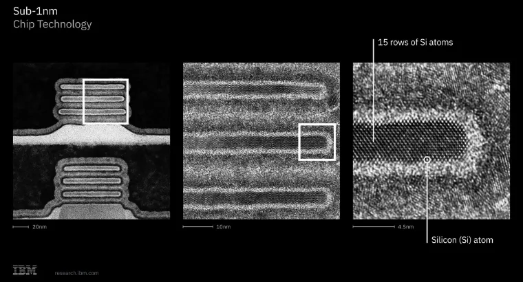
As per IBM, this change makes it feasible to optimise performance and efficiency at each level. The chip embeds nearly 100 billion transistors, which is almost twice the density of the 2 nm chip, which was launched in 2021. IBM said that this pattern was enabled by a combination of structural and material innovations, including its three-dimensional infrastructure.
Also Read: Musk Confirms “Starmind”, SpaceX’s Million-Satellite AI PlanIBM
Why the Breakthrough Matters for IBM Chip Scaling
IBM reported that the nanostar infrastructure was approved through a series of checks. These include ultrathin dielectric bonding, CMOS integration, bi-channel engineering capability, and functional CMOS in mortal operation with switching performance. External resources indicated by IBM at the VLSI 2026 conference show that the nanostar design can provide 40% scaling in static random access memory SRAM.
This change is intended to bolster the growing data bandwidth and effective requirements of advanced AI workflows. IBM’s semiconductor research facilities in the United States, including its Albany, New York site, are planning to host a High Numerical Aperture Extreme Ultraviolet (high-NA EUV) mechanism.
The semiconductor sector faces several issues as transistor dimensions reduce to the atomic scale. While chip nodes today refer more to manufacturing than accurate physical dimensions, moving below the 1nm wavelength has been viewed as a critical roadblock. IBM’s 0.7 nm technology, also known as 7 angstrom nodes, depicts a path ahead, accelerating logic scaling into the angstrom era.
By using a vertically stacked interconnect infrastructure, IBM states that the performance gains and efficiency can continue as more conventional planar scaling becomes less effective. Based on its present roadmap, IBM depicts that the nanostack approach could support at least another decade of transistor scaling.
IBM said that the sub-1 nm chip is expected to offer a 50% higher performance and 70% greater efficiency compared to its 2 nm node chips. If efficiently released, these gains could help workloads ranging from generative AI architecture to cloud computing infrastructure. While the chip remains a resource prototype, IBM has seen a path to prior production at scale deployment within the next five years.
IBM’s sub-1 nm chip, declaration highlight. Innovation in semiconductor research when the industry is struggling with conventional scaling. By launching a novel three-dimensional transistor infrastructure, the company emphasizes one potential for scaling developments in computing performance and efficiency. Although monetary deployment is far away, the work provides a significant insight into how future chips may be developed as the niche moves further into the angstrom era.